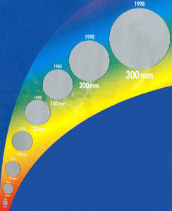
1964 : 25 mm
1969 : 50 mm
1974 : 75 mm
1978 : 100 mm
1982 : 125 mm
1985 : 150 mm
1990 : 200 mm
1998 : 300 mm
The fabrication of slices from pure silicon is based on a large set of steps that are presented in the following. The approach consists first to fabricate a crystal, precisely an ingot, which will be further cut in slices that will be transformed afterwards in wafers. To do this a lot of precautions have to be taken. Thus, these steps are numerous enough to build a full alphabet of elementary steps (after SCItec documents).
a) polysilicon load as pure as possible:
The purified silicon is used as load in the growth reactor. The main difficulty comes from the fact that the chemical quality, even high, remains low compared to the objective and to the doping concentration levels required.
Silicon crystal contains 5 x 10²² atoms per cm3. With a prity as high as 0.999999 (difficult to reach) the unintentional doping level can be in the range of 5 x 1016 cm-3. Some improvement is thus needed!
b) preparation of the load to melt the silicon and to transform it in ingot:
This load can be undoped or doped depending of the need for the integrated circuit substrate. Thus an additional doped silicon load, relatively well calibrated, is added to the global silicon load in the case of doped subtrates.
c) pulling of crystal ingot:
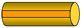
The first and more used technique is to pull an ingot of crystal from a seed. A silicon load, set in crucible (or melting pot), is melted. From a seed, well oriented, a progressive growth of the ingot following drastic conditions about temperature of the crucible, heating of the reactor wall, cooling of the ingot susceptor, temperature gradient along the ingot, heat transfer, pulling rate (speed), etc... The diameters of the ingot depend on the pulling rate; this method, presented figure 8, is called "Czochralski". Let us note that the difference of diffusion of species from the liquid phase to the solid one leads to modification of the relative concentration of species and more especially of doping atoms along the ingot. This aspect is very important because the resistivity of the final semiconductor ingot varies along this ingot. In other words, the final slices will have their resistivity position dependant: slices will be characterized and sorted for a range of resistivity, which can be up to the ratio three.
The evolution of the size of the ingots was linked to the process control and associated equipment. Because the goal is always to produce with higher efficiency, higher yield, and lower cost, the diameter of the ingots, and consequently of the slices, has been increased by a factor higher than ten for the thirty last years.
|
1964 : 25 mm 1969 : 50 mm 1974 : 75 mm 1978 : 100 mm 1982 : 125 mm 1985 : 150 mm 1990 : 200 mm 1998 : 300 mm |
|
Figure 7: Evolution of the size of silicon slices since the early integrated circuits.
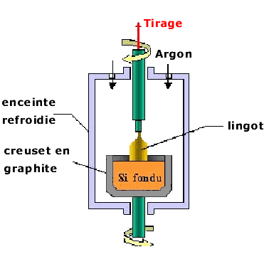
Figure 8: Pulling of an ingot from Czochralski technique. The diameter of the ingot is directly dependant of the physical process parameters..
Another technique can be used to fabricate large sized silicon ingots. It consists in starting from a polycrystalline silicon ingot got in the deposition reactor by reduction of trichlorosilane. Crystallization is performed by controlling the growth of the seed fixed at an extremity thanks to a moving of a "fused-zone" (noted "FZ"). This zone is heated at a temperature just under the fusion point by a high frequency power supply via a coil surrounding the ingot (Foucault's current effect).
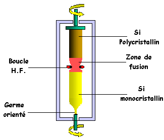
Figure 9: Crystallization of a silicon ingot and associated purifying using fused-zone technique. During the moving of the fused zone, the doping atoms and impurities are redistributed in the ingot. This technique is used to fabricate high purity semiconductor slices
This FZ technique is also involved for purifying the ingot ; the principle is to take benefit of the difference of diffusion of species at high temperature in a crystal. In this case, up to three coils are set in the qsystem to save time. This technique allow fabricating very lightly doped ingot very usefull for high power devices or high voltage integrated circuits(quasi-intrinsic zones allowing high voltage strength).
Another technique can be used to fabricate ingot,and is specially devoted to III-V coumpound semiconductor. The load is set in a paralelipipedic susceptor, the lower part being circle shaped. The crystallization process is managed by controlling the heating of the several species. For such semiconductor the partial pressure of the more volatile specy is very high at the process temperature (for example, more than 30 bar for phosphorus in the case of InP). This technique is called "Bridgman". Figure 10 gives a simplified description of this technique.
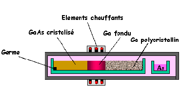
Figure 10: Ingot pulling using Bridgman technique. This technique is more especially devoted to III-V compound semiconductors such as GaAs or InP.
d) Ingot cropping:
This operation consists in cutting, or cropping, the extremities of the ingot, which are the high defect concentration regions with a variable diameter.

e) control of the resistivities on the top and bottom faces of the ingot:
Due to the variation of the doping concentration during the pulling, the final resistivity varies in function of location. A check of resistivity and an agreement with specifications are needed. A four probe method equipment makes these measurements.
f) crystallographic orientation of the ingot:
To check the cristallographic quality but also to detect the effective reticular plans to select the cutting axes, crystallographic analyses are clearly useful; they are based on X-ray diffraction technique. One or two flat zones on the edge of the ingot are processed to get a crystallographic orientation reference for the wafer fabrication. Don't forget that the final cutting of the dies are performed paralelly to a crystalographic plan of the lattice (plan <100> for example).
g) cylindrical polishing:
During the pulling, due to the very large set of physical parameters to control, in fact the diameter of the ingot slightly varies that creates some waves at the ingot surface. To get slices of calibrated diameter suitable for automatic equipment, a cylindrical polishing is needed.
h) polishing of the flat line to get geometrical and crystallographic reference:
This reference will be used during the wafer process (orientation of conducting zones, detection of motives during photolithography setp, crystallographic axes for the die cutting). In addition, depending on the doping type of the substrate and its cristallographic orientation, additional repears are processed on the edge of the ingot and thus of the slices. A code is thus defined as shown figure 11. On can notice that on the 200 mm diameter slices, only a small trench is processed: type and nature of substrate are, in this case, laser printed on the suface of the future slice.
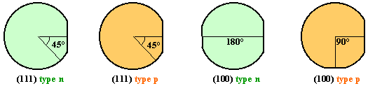
Figure 11: Identification flat zone of slices. n-type and p-type slices as well as surface crystallographic orientations are simply identified.
i) ingot sawing :
This sawing is proceeded with a diamond tooth saw about 400 µm thick.
- saw is about 400 mm thick, that means creation of an equivalent thickness of powder!
- slice thickness 400 µm to 600 µm thick just after sawing, and thus not quite different of the powder transformed part!
Accounting cropping, sawing, and polishing more than 50% to 60% of the ingot is "destroyed". In practice, the slices at least 150 mm diameter are at least 500 µm thick during the circuit process in order to avoid mechanical weakness. This thickness is drecreased to 250 - 300 µm before cutting in dies in order to make easier the thermal exchange with the chip carrier in the final packaging.
j) thermal treatment:
The sawing creates mechanical stresses in the crystal. The crystal needs thus some treatment to decrease the constraint number. A high temperature thermal treatment, called an "annealing", is then processed at about 600°C to 700°C. At these temperatures, the atom energies are high enough to give them some mobility that allows them joining the substitutional position in the lattice.
This thermal treatment gives also advantage to decrease the oxygen effect (donnor-like type) as well to stabilize the resistivity.
k) polishing of the edges:
After sawing, some "peaks of matter" remain on the peripheral zones of the slices. One has to remove them. In addition, to make easier the manipulation of the wafers during the IC's fabrication process, a circle shaped edge is proceeded; this avoids the degradation of the wafer transfer equipment but also creating cracks, or dislocations in the crystal, which lead to definitive brakes.
l)sorting of the slices in function of the thikness:
The thicknesses after sawing can be significantly different. To decrease the cost, the quantity of matter to grind has to be minimized. Usually, the wafers are sorted by thickness range of ten micrometers (10 µm).
m) overlapping of slices with an alumina mixture - polishing:
In order to improve their surface quality, the slices are polished using a mixture that contains alumina or diamond grains for which the size is about several micrometers. The slices are set in a polishing machine as shown figure 13.
n) cleaning:
This step consists in removing the abrasive species and contaminants by solvant etching and ultra pure desionized water rinsing.
o) chemical etching of the slices:
During the previous steps, a native oxide grows at the silicon surface; this native oxide contains impurities either metal based or organic based. These impurities are respectively removed by an acid solution etching and a basic one:
- acid solutions: HNO3, CH3COOH,
- basic solutions: KOH. Sodic solution (NaOH) is not used because sodium is a strong contaminant for the oxides and more especially for the gate oxides of MOS transistor gates.
The native oxide is finally etched by a fluorhydric acid solution (HF) and rinsed in desionized water. The surface is then chemically neutral before "mirror" polishing.
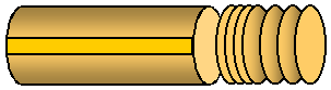
p) damaging of the back side:
The useful part of the slice is in fact really close to the upper side. The main goal is to give to this zone a quaility level as high as possible concerning as well the impurity content as crystallographic defects (dislocations twins, etc...). The effective process consists in creating defects on the back side of the slice by sanding or laser beam insolation that induces a depolishing. During the folowing thermal treatments, the impurities located to the front side migrate to the back side and are trapped by the induced defects thanks to their energy levels more easily reached by the impurities, as shown in figure 12. This phenomenon is called "gettering".
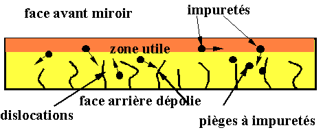
Figure 12: The back side of the slice is damaged. It loses itas mirror aspect. This operation allows improving the effective active zone of the final circuit very close to the upper face.
q) sort in function of thicknesses:
After back side damaging, the thicknesses are modified and a new sort is performed.
r) preparing the polishing of the active face:
The slices are mounted in polishing machines as shown figure 13.
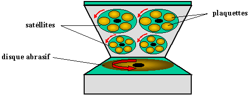
Figure 13: The slices are mounted in a polishing machine. These machines are designed with satelittes turning on themself in order to improve the homogeneity of polishing (after SCItec documents).
s) grinding of the thickness excess:
about 25 µm are grinded.
t) final "mirror"polishing:
This polishing can be mechanical or chemico-mechanical based. Straights and orange skin have to be
suppressed. This operation is performed with the same equipment than this presented figure 13, but the polishing solution
is less agressive with a mixture containing smaller grains of alumina or diamond. The grain diameters can be as low as
0.1
u) cleaning and sorting:
These last operations allow:
- dismounting the slices from their polishing susceptor,
- final cleaning,
- final sorting in function of thicknesses.
v) resistivity test, final sorting in function of resistivities:
In order to prepare the customer lots, a sort in function of resistivities is performed.
w) writting:
The writting of the lots mentionning ingot number, date, etc.. , is performed through a laser beam scanning. These indications will allow controlling each wafer during the fabrication process of circuits and devices.
x) final cleaning in cleanroom:
To start the fabrication process of the circuits, any contamination has to be rejected, no dust, no fat film, no organic deposit. A final cleaning is thus needed and performed in an ultra-cleaned ambiance.
y) visual inspection:
The human eye remains the best visual inspector. It detects variations of colour, straights, pits, raies, and submicronic sized dust. An optical scanning automatic system testing all the slices can not be suitable and performant enough. As an example, let us consider a tested surface of 10 cm x 10 cm needing a scanning pixel of 0,05 µm x 0,05 µm .
An analysing pixel 0.05 µm x 0.05 µm needs at least 1 µs of computing real time treatment (spectral analysis). In this case, the total testing duration is:
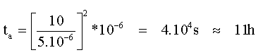
This is a huge duration and not suitable. In fact, in this case, the eye is much more efficient because it treats a lot of informations in parallel, thanks to millions of retinian cells! Thus it remains competitive!
z) flatness test:
This test is important for the lithography step in order to well focuse the insolation beam at the surface of the future wafer. Some equipments are specialy designed to make this measurement; they are based on the deviation of a laser beam.
After all these steps, the slices are ready to be processed for fabricating integrated circuits (or discret devices). In the following, the slices are called "wafers" due to their physical aspect!
BEGINNER
>> 
ADVANCED
>> 
![]()