- molecular beam epitaxy or MBE,
For each technique, specific equipment are involved.
This technique consists in sending atoms or molecules at the surface of the substrate in an ultra high vacuum in order to prevent any contamination and the collisions along the path. Thee principle of the source is evaporation under vacuum with Knudsen cells by well controlled heating. The evaporating sources may be of several types; for each evaporated material, the heating must be specific to well control the material flux towards the substrates. From this control, a n atomic or molecular beam is produce in direction of the susbstrates. With a low flux, the growth can be very well monitored and the crystal can be grown atomic layer by atomic layer. By changing the nature and/or the doping of the material some very complex structures may be fabricated such as super lattice, laser diodes or high electron mobility field effect transisotrs (HEMT). Thus one can obtain a very good growth definition, abrupt junctions but this technique is very long, only one substrate is processed. The growth rate is in average 1nm per minute. As a consequence this technique is very expensive and is reserved for the fabrication of devices with a very high added-value.
This ultra-high vacuum system, 10-10 Torr, allows all types of in-situ control techniques and all in-situ characterizations for which a high vacuum is required: electron diffraction, Auger spectroscopy, Electron Spectroscopy for Chemical Analysis-ESCA (XPS ou UPS), X-ray diffraction, etc... All along the process, the crystallinity of the grown layers can be checked.
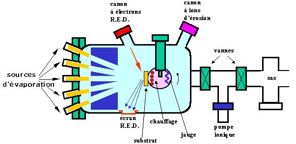
Figure 16 : Molecular Beam Epitaxy reactor or MBE (After D.V Morgan et K. Board [3]).
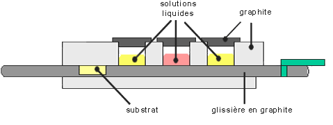
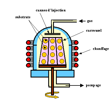
Liquid phase epitaxy
This technique consists in growing the crystal from the contact between the substrate and a liquid source of the materail to grow. The priciple is really similar to the Czochralski ingot pulling method. The thermal exchanges have to be very well controled in order to avoid a melting of the substrate crystal. This technique has the great advantage to be very fast, the growth rate being as high as several microns per minutes. However, the accuracy of the concentration profiles of species is much lower than the MBE one.